High Voltage Power Supply for Nixie Tube Projects
Overview
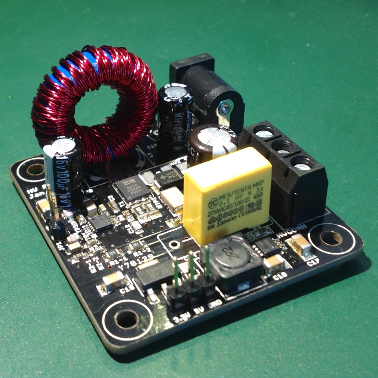
This project is a HVPSU (High-Voltage Power Supply) that generates up to 220V from a 12V input. In addition to that, it also provides 2*Vout (so, up to 440V, for dekatrons), and two outputs for powering digital logic: 5V and 3.3V. The primary HV boost circuit reaches 88% efficiency when going from 12V to 185V at 55mA, with a 3% output ripple.
I designed it because I couldn't find anything that would make sense for my Nixie projects. There are plenty of tiny power supply modules available on eBay, but most of them end up being impractical: no 3.3V (for my microcontroller) and 5V (for my 74141 nixie drivers), no mounting holes, no >400V output for powering dekatrons. Some supplies make a token gesture towards practicality by sticking a 7805 on the same board, but you quickly find out that the current draw of 6x74141 is enough to require a large heat sink on a 12V-powered 7805 (one 74141 consumes 12.5mA!). This means that instead of a single-board power supply you end up routing your input power all over the place, implementing your power supply in several places.
I wanted to have something versatile enough so that I could use it in a number of projects: with nixies, dekatrons, other tubes, VFDs, phone ringers, etc. I also wanted it to fit on a 5x5cm PCB, so that I can order 10 PCBs for $10 at iteadstudio.
The version I'm posting online is not perfect, but works quite well in a number of my projects. I decided I'd rather publish it as it is now rather than keep it locked forever.
The circuit and PCB you see are the result of multiple iterations. I started out with a design based on MAX1771, which turned out to have stability problems, mostly due to EMI on the feedback pin. I then went through seven board designs, trying to make it work. I ended up with a design that mostly worked, but exhibited uncontrolled behavior in some conditions (load transients, overcurrent, EMI). I finally got tired of the MAX1771 chip and decided to look for another solution.
I chose the TPS40210 from Texas Instruments, which seemed to be a solid performer in high-voltage boost applications, was easily available, not too expensive. The existence of an automotive-grade version also means that the chip won't disappear anytime soon. I went through three board revisions with the TPS40210, which were mostly about shrinking the design and adding the TPS62160 buck converter instead of a 7805 to produce 5V.
In the process I learned a lot and discovered that there is a lot of stuff about boost converters that I didn't even know I didn't know. Here are a few examples:
- Loop stability: I had no idea why it was an issue or how to design loop compensation (TI's SwitcherPro is really helpful).
- CCM vs DCM and transitions inbetween.
- Current-mode control sub-harmonic instability in continuous conduction mode.
- RC snubber: do you know about parasitic ringing on the switching node? That ringing that your scope probably won't show, because it's above 500MHz?
I now know slightly more, but the circuit certainly isn't perfect. I don't even have the equipment to measure some of its properties, so I have to leave it as it is.
There are two principal reasons for making this available as an open-hardware project:
- I learned a lot by studying the designs of others, and I felt I owe the community something in return (Nick de Smith's Nixie HV Switching PSU page was especially helpful).
- Most Nixie PSU designs I saw online are based on the MAX1771, and apart from people hacking crude 555 supplies, there seems to be little variation. I thought an alternative should be out there.
Features:
- Generates 4 voltages from 12V input:
- Vout: up to 220V at up to 80mA, 2-3% voltage ripple
- 2*Vout (optional): up to 440V at up to 30mA
- 5V at up to 1A at ~85% efficiency for older digital logic such as 74141 Nixie drivers (compare to about 40% efficiency if a 7805 is used)
- 3.3V for modern digital logic (microcontrollers, etc)
- High-voltage DC-DC converter can be shut down digitally to save power
- Can be used with many different power inductors, depending on desired output power:
- SMD 12.5x12.5mm
- THT vertical barrel type, rasters of 5mm, 8mm, 11mm
- THT vertical toroidal type, 8mm raster, up to 23.5x11mm
- Known & fixed switching frequency (50kHz)
- Nominal input is 12V, can be up to 16V
- Safety features: overcurrent protection, thermal shutdown, slow-start.
Downloads, Release Notes and Licensing
- Schematic as a PDF file
- A zipfile containing the schematic, PCB, Eagle .sch and .brd files, and Gerbers prepared for manufacturing at iteadstudio.
- There is also a partlist, as generated by Eagle. Not a real BOM, but at least you'll know what to need and what resistor sizes to use.
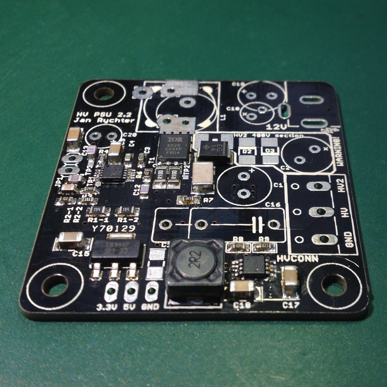
Version 2.2 is what I use in all my projects. Version 2.3 has several tiny fixes: adjusted position of mounting holes, added comments in the schematic, but is otherwise identical to 2.2.
I wanted to pick an Open-Source Hardware license, but couldn't find one. There is lots of talk about Open-Source Hardware, but when you actually want to open-source something, it turns out it isn't easy.
So, to make it clear: this design (this includes the schematic, PCB design, and the output gerbers) is available for anyone to do whatever they want with it. Take it, modify it, make money with it, heck — even sign your name on it if that fits your moral guidelines.
Design assumptions:
- Wide range of output voltages for various HV projects: from 60V for VFD displays to 440V for dekatrons
- Wide range of output currents: from single mA up to 80mA at 180V for large numbers of nixies
- Should also supply 5V and 3.3V for digital logic with good efficiency
- Good transient response for nixie multiplexing, PWM dimming, or IN-9/IN-13 bargraph displays
- Stable behavior from no load to maximum load, over entire supported Vin range
- Fixed switching frequency so that noise/interference is more predictable
- Must tolerate various inductors, as those are hard to get and some types might be expensive in parts of the world
- Must not use a transformer, for the same reasons
- Should accomodate slight variation in components where possible
- Should be reasonably quiet: EMI should be limited, predictable and well-behaved
Things I didn't care too much about:
- Board size: you could make the board much smaller by removing optional areas, 5V and 3.3V voltage generation, ARK connector for HV output, 12V DC input connector, and mounting holes. But if you do that you end up with a cute, but completely impractical board. There is no point in making the PSU tiny, as Nixies are not small. You normally have lots of room.
- Cost: actually, I did care about cost. But anything listed in the "design assumptions" above had precedence. Using a 7805 instead of the TPS62160 is definitely cheaper, but you end up with lots of dissipated heat/power and a large heatsink. Same goes for the FET: yes, you could use an IRF644, but efficiency and EMI would suffer.
All of the following graphs and calculations assume a switching frequency of 50kHz, Vin=12V, Vout=180V, RdsON=100mΩ and L=47µH, unless stated otherwise.
Modifications
In general, before you modify anything, I'd suggest reading the datasheet for the TPS40210 carefully.
Some aspects of the design are easily adjustable:
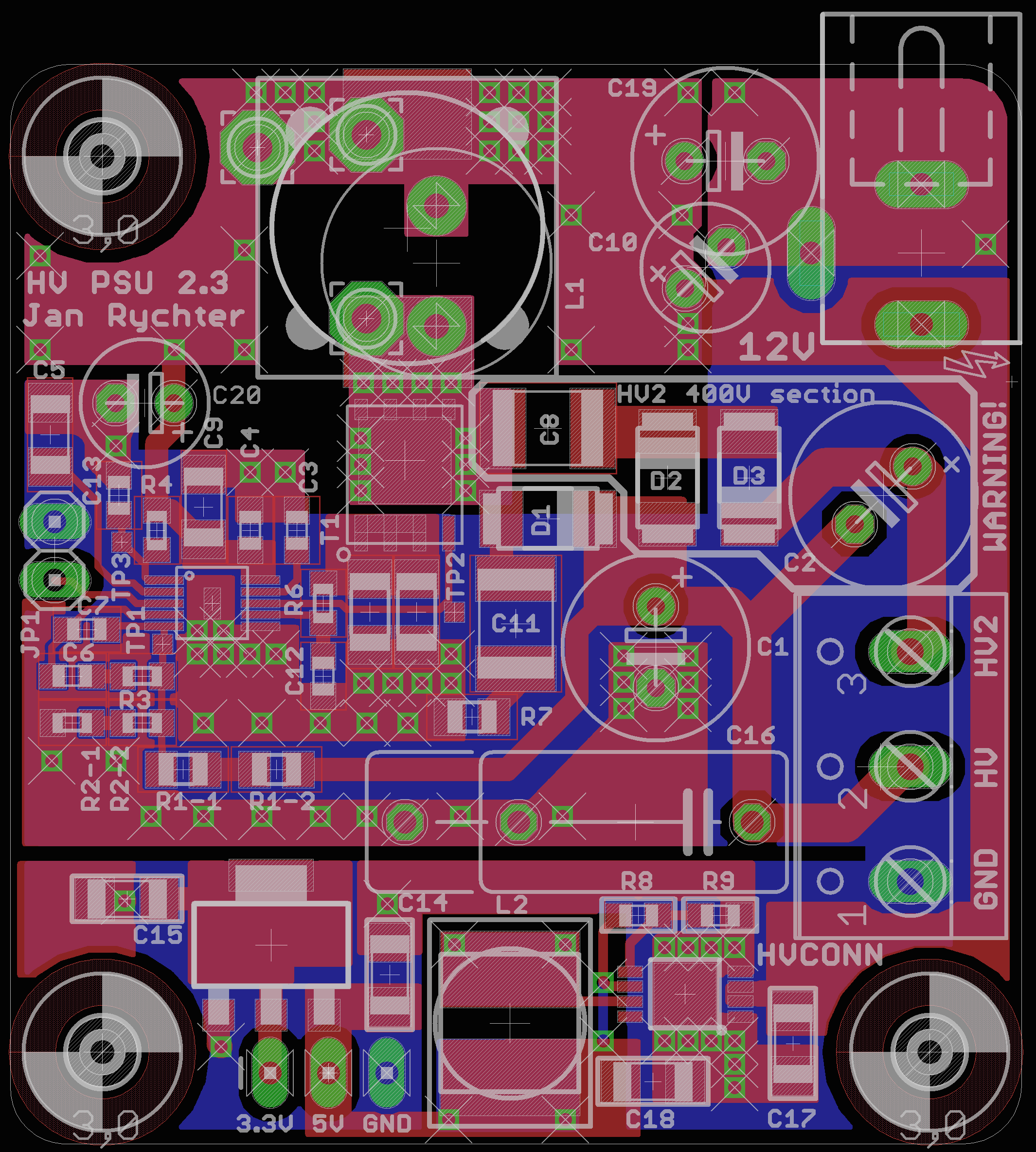
- To adjust the primary output voltage, change R1-1 and R1-2. These, in conjunction with R2-1 and R2-2 form a divider that decides what the output voltage will be.
- If you don't need some of the output voltages, just don't populate the corresponding part of the board. For example, if you don't use dekatrons at more than 400V, don't populate C8, D2, D3 and C2.
- If you don't need 5V, but do need 3.3V, change the resistor divider next to the TPS62160 (R8/R9) so that the chip generates 3.3V directly, and leave out the 1117 stabilizer.
- C20 and C14 are optional and I don't actually use them in my builds. The space is there so that you can experiment and if you need them, you can add them.
Design Notes
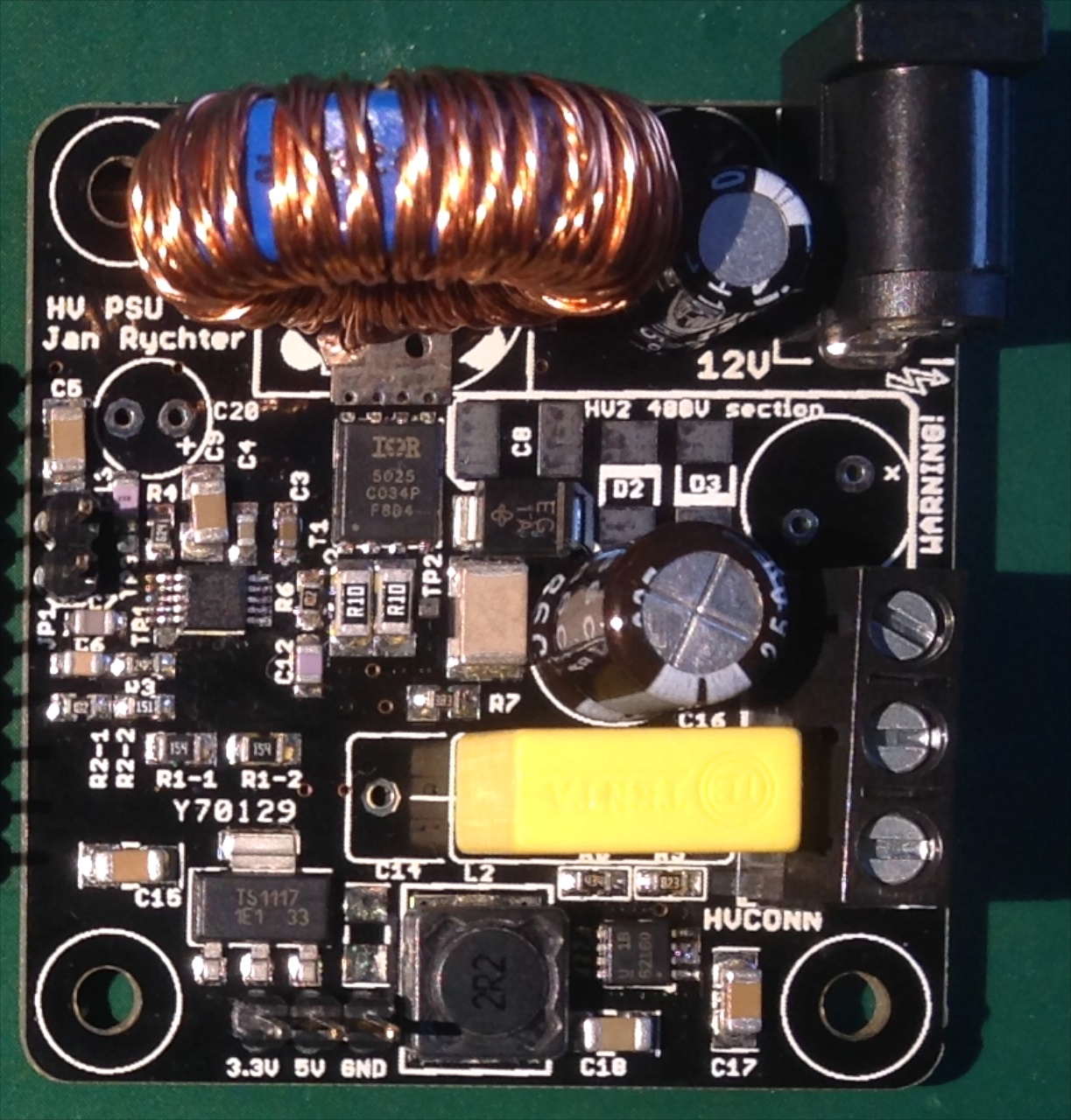
Inductors
The power inductor you choose is the single most important factor that affects the efficiency. I experimented with many inductors, finally settling on a large toroidal (either DTMSS-20-0,047/6,0-V or DTMSS-20-0,068/4,0-V from Feryster). If your design is space-constrained, use a shielded SMD inductor like EPCOS B82477P4473M000 (47µH, 2.8A) or Coiltronics DRA127-470-R (47µH, 2.3A), but efficiency will suffer, and you will be limited with your output current.
Take care to read about peak inductor current in the TPS40210 datasheet if you want to go to higher output currents. If you're powering 6 IN-12 Nixies, you only need about 15mA, but 6xIN-18 will put you at almost 40mA max current.
The peak inductor current in a boost converter depends mostly on input voltage, output voltage, switching frequency and inductor value. To understand the peak inductor current, I made the following graph. This is the peak inductor current for Vin=12V, Vout=180V, plotted for various inductor values and a range of output currents:
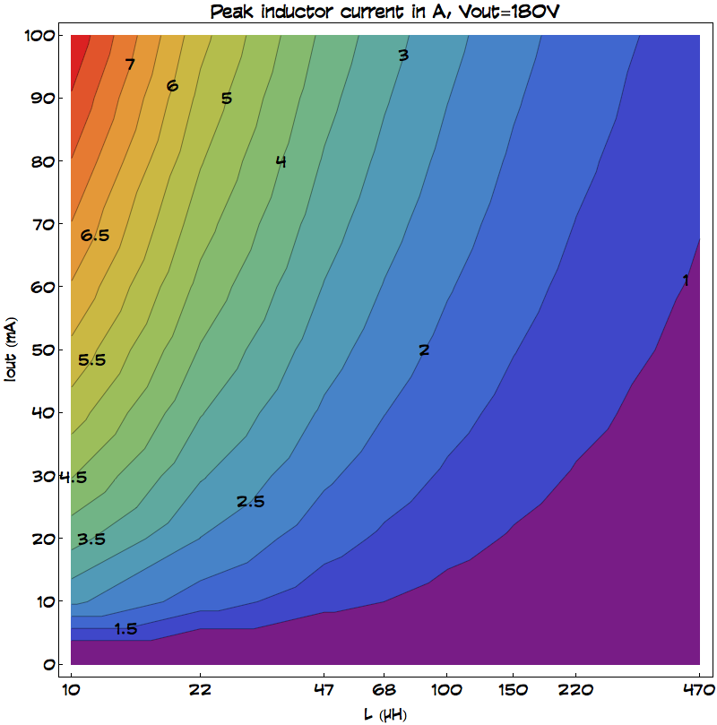
As an example, with a 47µH inductor and 15mA output current, the peak inductor current is between 1.5A and 2A, so if we choose an inductor with a saturation current of 2A, we should be fine.
I would not advise using an unshielded inductor, unless it's a toroidal one. The electromagnetic field will be quite strong and you might have problems with EMI.
As for L2, it should be a shielded 2.2µH SMD-mounted inductor. I used a generic MCSDRH73B-2R2MHF from Farnell (7.3mm x 7.3mm). The footprint is designed to be very flexible, with large pads that can accomodate almost any 2.2µH SMD coil up to 7.5mm x 9mm. See the TPS62160 datasheet for details on the peak inductor current.
Current Sense Resistor
You will notice that there is space for two current sense resistors (R5-1 and R5-2). There is a practical reason for it: it will often be easier and cheaper to obtain two lower-power resistors then a single large-power one. Also, the larger power resistors come in non-standard packages.
As an example, instead of using a single 50mΩ resistor, I can use two 1206 100mΩ 0.33W resistors connected in parallel.
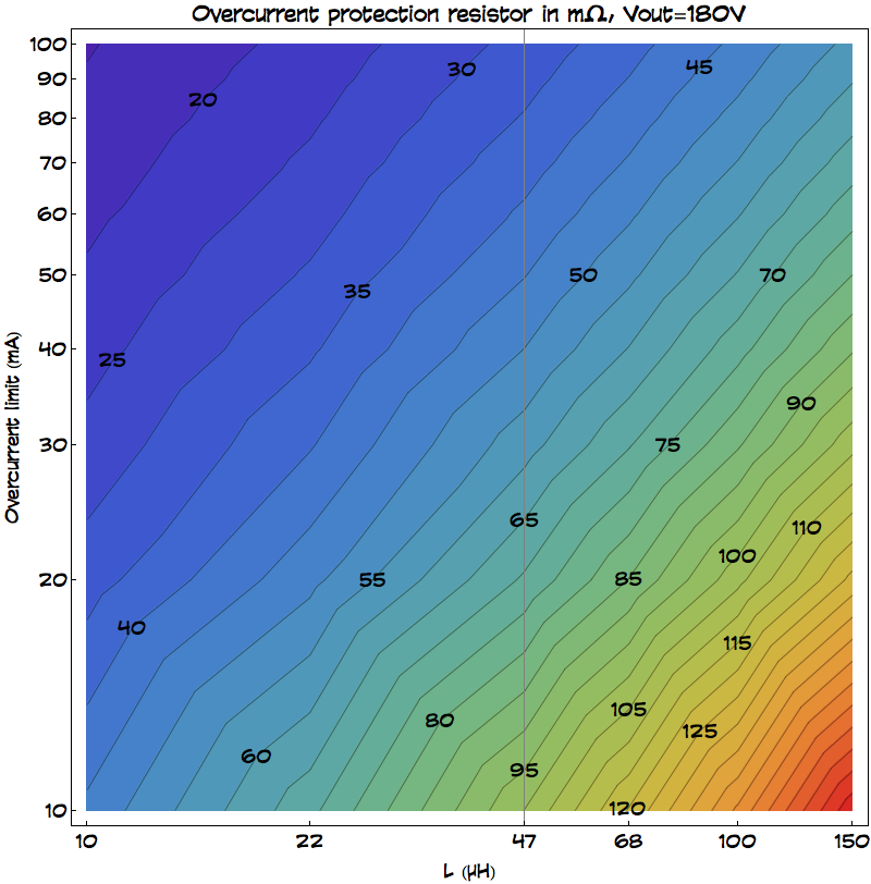
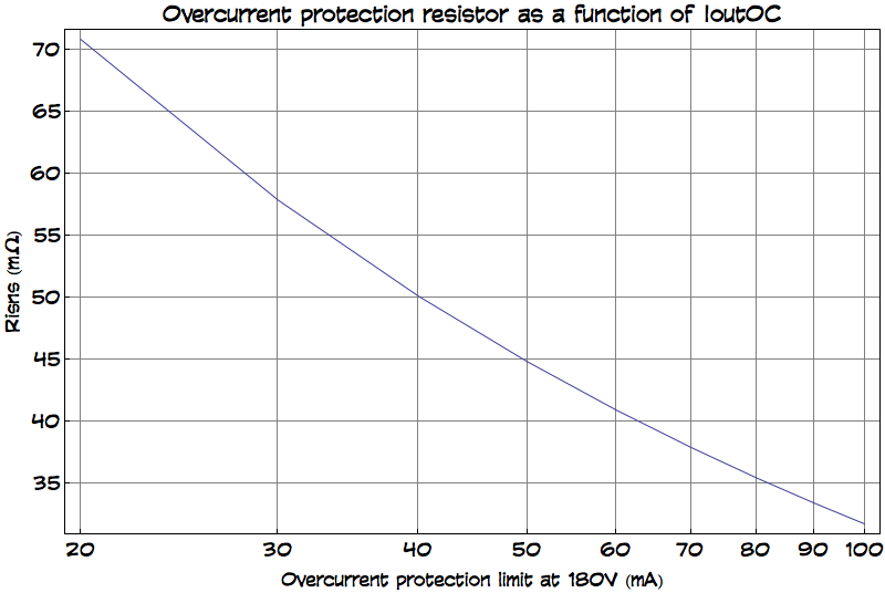
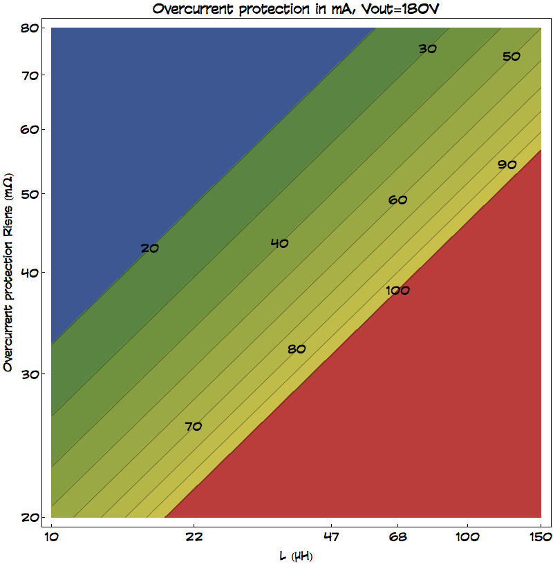
The current sense resistor actually serves two purposes: one, as the name implies, is to sense and measure the current flowing through the inductor and MOSFET. The second purpose is to provide overcurrent protection. The exact formula to compute the appropriate value of Rsense should be taken from the TPS40210 datasheet, but the graphs should give you a better idea of the tradeoffs and reasonable values.
Switching MOSFET
I don't recommend changing the switching MOSFET (IRFH5025TR2PBF). It has been carefully chosen and has excellent parameters. It barely even gets warm in normal operation, and the PCB provides adequate heatsinking. The only worrying thing is its VdsMAX of 250V, which leaves little headroom if you're generating 180-200V and allow for inductor spikes. The RdsON of 100mΩ is very good for a 250V MOSFET (that's 3x better than the commonly used IRF644!).
In projects that have lower voltage requirements (VFD, ringers, etc) you might consider the IRFH5207TR2PBF. It has the same footprint, VdsMAX of 75V and RdsON of just 9.6mΩ. If you're going for 60V output, this could be an option.
Maximum Output Current
So, what is the maximum output current for this design?
This is something I can't really answer. I wasn't able to hit the limit (I tested up to 80mA at 185V). The practical limitation is the inductor you choose and its maximum saturation current (see the graph showing the peak inductor current). For 100mA output at 180V you will be hitting 3.5A-4A with a 47µH inductor. The IRFH5025 MOSFET can handle up to 32A and the PCB should not have any problems dissipating the heat, but you will need a large toroidal inductor and you might run into other issues, such as input voltage dropping, insufficient input capacitance, or (if you increase the input caps) large inrush current at power-on. I also don't know how a generic output capacitor will behave with large currents: it might heat up unacceptably. So I can't really answer that question, and I'd be curious to find out myself.
Operating Frequency
The PSU operates at around 50kHz (actually, sometimes even slightly below that, but don't tell anyone, as the TPS40210 specifications mention 50kHz as the lower limit). Normally one would use a higher frequency, but with such a high output voltage the MOSFET gate charge becomes a significant source of switching losses. My measurements showed that going above 50kHz does indeed quickly lead to a drop in efficiency, losing already ~5% at 76kHz.
Voltage Doubler
C8, D2, D3 and C2 form a voltage doubler that provides 2x Vout. You may leave this area unpopulated if you don't need it. Be aware that this output is unregulated — it will follow Vout, but you will get at least double the ripple, and it won't respond to load changes as well as Vout. It should not be used as a primary output. It's fine for biasing dekatrons, but don't expect much more from it.
Split Resistors
You might have noticed that R2 is split into two 0805 resistors. Similarly, R1 also has two places reserved (0603 this time). There main reason for doing this is that R2 will have nearly the full output voltage across it. To avoid getting high-voltage rated resistors, we use two resistors in series, thus dropping the voltage across each resistor by half. I also used 0805 resistors here, because they will likely have a higher voltage rating.
In practice, you won't even get the voltage rating for most cheap resistors, so this is a guessing game — but we are stacking the odds in our favor.
As for R1, the reason for splitting it is so that you can get the resistance you need from the components you already have.
Output Capacitor
C1, the output capacitor for the boost converter, forms an integral part of the converter loop. Normally, one would carefully pick a low-ESR capacitor, design loop compensation based on that particular part, and measure the loop response with a network analyzer using a transformer-injected signal. But this being a hobby design I have no such luxuries. The output cap has to be rated at (at least) 250V, which really limits the choice, especially if you also want the price to be reasonable. And it is likely that every build of this design will use a different cap in this place. So I've made certain assumptions, which should hold for reasonable 4.7µF/250V electrolytics. If possible, use a cap with lower ESR, but overall it should make little difference.
C16 is a filter capacitor. It is optional, but very nicely filters the output ripple, so I use it in every build. It's a 100nF MKT cap in a rectangular-footprint package and the PCB allows for two raster sizes: 10mm and 15mm.
Potentiometer (or rather the lack of it)
Note that there is no potentiometer, so the output voltage is not adjustable. This is not by accident. I found that vertically-mounted precision pots (and you do need a multi-turn precision pot for any meaningful adjustment) make great antennas for picking up EMI from the primary inductor. The feedback pin is very sensitive to noise, so any interference will make the circuit unstable or prevent it from working at all.
I decided that one usually builds a PSU for a specific project with a fixed voltage anyway, and in the worst case it isn't that difficult to desolder and replace R1/R2.
Case Variants
The primary inductor and some capacitors have space reserved for multiple case variants. This is because these components are difficult to get in standardized packaging and it's likely people will use many variants. The footprints might look strange (and the double inductor symbol in the schematic looks weird, too), but it's very practical.
Snubber
The RC snubber is formed by C11 and R7. I have no way of testing whether it does the job correctly, as I only have a 100MHz scope. I followed the recommendations from Texas Instruments (the Switcher Pro application), and I can only hope it helps.
Enable Pin
Do not forget to place a jumper on JP1. If the enable pin is left floating, you might end up with the boost controller disabling itself. TPS40210 has an internal pulldown resistor on the enable pin, but it is very weak (1.1MΩ).
If you control the enable pin with external digital circuitry, pulling the enable pin above 1.2V shuts down the boost controller. This will not shut down your digital supplies (5V and 3.3V), however.
Because of the slow-start feature of the TPS40210 this input isn't really amenable to PWM.
Continuous Conduction Mode vs Discontinuous Conduction Mode
A circuit with an inductor can operate in one of two primary modes: CCM (Continuous Conduction) or DCM (Discontinuous Conduction). The difference is that in CCM current flows through the inductor all the time, while in DCM current falls to zero during a part of the switching cycle.
In general, it is preferable to be in CCM, as the peak current will be smaller, you will place less stress on the components, and because of smaller peak currents, EMI will be less of a problem. However, staying in CCM requires maintaining certain output current. If your output current falls, you will end up in DCM. There are a number of variables that affect whether you are in CCM or DCM, so I made some graphs to better visualize and understand the transition boundaries (see below).
All datasheets for boost controllers will provide different sets of calculations for CCM and DCM. I have never seen a discussion of CCM/DCM transitions and it seems to me this topic is generally avoided. In our case, it is difficult to avoid it, because we do not always know what the actual load current will be, and if you use PWM for Nixie brightness control, your output load will vary wildly.
An additional problem that occurs specifically in current-mode controllers operating in CCM is sub-harmonic instability (see pages 15 and 16 of the TPS40210 datasheet). While I managed to understand the reason for this problem, I never understood what the solution is. And because in the case of this circuit the maximum allowable Rsense (R5) value to avoid instability is 6mΩ, and my experiments showed that I am indeed getting unstable behavior (controller skipping cycles, lowering efficiency), I decided to design the circuit to stay in DCM all the time.
Here is a graph showing the transition boundaries between DCM and CCM at 50kHz, for Vout=180V, for various inductor values (given in µH):
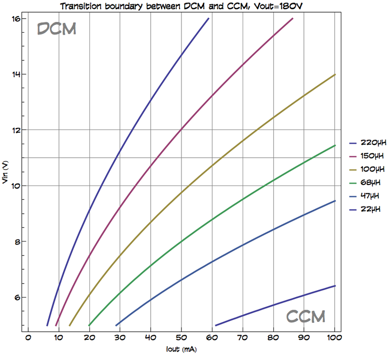
Note for example that with a common 100µH inductor size, if one pulls 60mA from the output, Vin falling below 11V will make the circuit go into CCM. I discovered it the hard way: my crappy Chinese power supply indicated 12V, but it turned out to be just chest-thumping, as under load the voltage fell below 11V, even though the display said 12V. Don't trust your power supply.
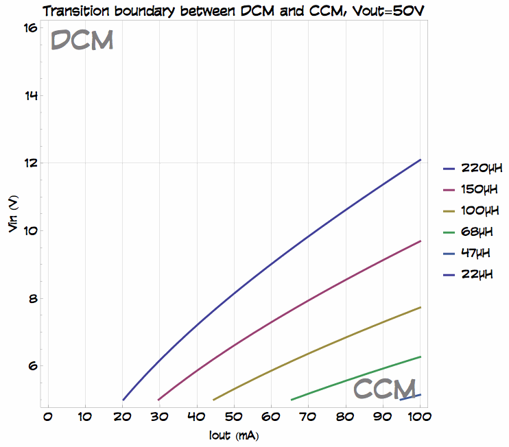
To better understand the transition boundaries between DCM and CCM, take a look at the following graph/animation. It illustrates transition boundaries between DCM and CCM at 50kHz, for various inductor values and for various Vout values. Note that the bigger your output voltage and output current are, the more likely you are to end up in CCM:
I decided to go with a 47µH inductor. That value means that even if my input voltage falls to 11V, I can safely go up to 220V at 80mA without entering CCM territory (and thus encountering instability).
Things To Do
There are things I would like to do, but lack either the time, or equipment:
- Use a network analyzer to measure the loop performance (I don't have access to a network analyzer).
- Measure transient response using a load tester (building a load tester capable of sinking 80mA at 220V is a project in itself).
- Perform exact efficiency measurements (mine are just approximations).
- Figure out a practical solution to the current-mode control instability in CCM, which would allow going into CCM (if anybody understands this, I'd be glad to learn!).
- Measure the RC snubber and possibly improve the component choice.
For now, I'm leaving the design as it is — it works well enough for me.
Thanks To
- Nick de Smith, whose excellent Nixie HV Switching PSU page got me started and served as an example of how to publish your work so that others may learn from it.
- Helpful people in the neonixie group — this is a good place to learn, you will get lots of friendly and helpful advice.
- Texas Instruments engineers helpfully responding in the E2E forums.
Revision History
This page was first created on 2014-05-04.
Comments
If you'd like to add a comment or discuss, see the corresponding blog post. Or just write to me directly.